(China (Mainland))

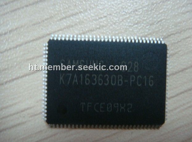
Product Summary
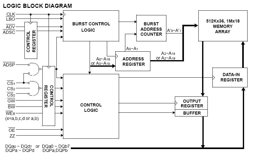
The K7A163630B-PC16 is a 18,874,368-bit Synchronous Static Random Access Memory designed for high performance second level cache of Pentium and Power PC based System. The K7A163630B-PC16 is organized as 512K(1M) words of 36(18) bits and integrates address and control registers, a 2-bit burst address counter and added some new functions for high performance cache RAM applications; GW, BW, LBO, ZZ. Write cycles are internally self-timed and synchronous. The K7A163630B-PC16 is fabricated using SAMSUNG’s high performance CMOS technology and is available in a 100pin TQFP. Multiple power and ground pins are utilized to minimize ground bounce.
Parametrics
K7A163630B-PC16 absolute maximum ratings: (1)Voltage on VDD Supply Relative to VSS VDD: -0.3V to 4.6V; (2)Voltage on VDDQ Supply Relative to VSS VDDQ: VDD V; (3)Voltage on Input Pin Relative to VSS VIN: -0.3V to VDD+0.3V; (4)Voltage on I/O Pin Relative to VSS VIO: -0.3V to VDDQ+0.3V; (5)Power Dissipation PD: 1.6W; (6)Storage Temperature TSTG: -65℃ to 150℃; (7)Operating Temperature Commercial TOPR: 0℃ to 70℃; (8)Industrial TOPR: -40℃ to 85℃; (9)Storage Temperature Range Under Bias TBIAS: -10℃ to 85℃.
Features
K7A163630B-PC16 features: (1)Synchronous Operation; (2)2 Stage Pipelined operation with 4 Burst; (3)On-Chip Address Counter; (4)Self-Timed Write Cycle; (5)On-Chip Address and Control Registers; (6)VDD= 2.5 or 3.3V +/- 5% Power Supply; (7)5V Tolerant Inputs Except I/O Pins; (8)Byte Writable Function; (9)Global Write Enable Controls a full bus-width write; (10)Power Down State via ZZ Signal; (11)LBO Pin allows a choice of either a interleaved burst or a linear burst; (12)Three Chip Enables for simple depth expansion with No Data Contention only for TQFP ; 2cycle Enable, 1cycle Disable; (13)Asynchronous Output Enable Control; (14)ADSP, ADSC, ADV Burst Control Pins; (15)TTL-Level Three-State Output; (16)100-TQFP-1420A (Lead and Lead free package); (17)Operating in commeical and industrial temperature range.
Diagrams